Introduction
For decades, silicon has powered the digital world. Every smartphone, laptop, and data center depends on silicon-based chips. However, as silicon approaches its physical limits, the semiconductor industry is searching for the next breakthrough.
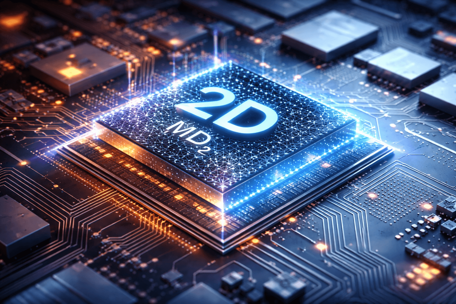
Now, a major development in 2D semiconductors suggests that the future may lie beyond silicon.
Recent research led by the Chinese Academy of Sciences (CAS), along with Peking University and Tsinghua University, has demonstrated a critical advancement:
The ability to grow ultra-thin semiconductor materials at wafer scale with high speed and precision.
This breakthrough in 2D semiconductors could mark the beginning of a new era in computing.
What Are 2D Semiconductors?
2D semiconductors are materials that are only a few atoms thick. Unlike traditional silicon, these materials maintain excellent electrical control even at extremely small scales.
One of the most important materials used in this research is:
- MoS₂ (Molybdenum Disulfide)
This material belongs to a class known as Transition Metal Dichalcogenides (TMDs) and offers several advantages:
- Atomic-level thickness (~0.7 nm)
- Strong control over electron flow
- Low leakage at nanoscale
- Natural bandgap for efficient switching
These properties make 2D semiconductors strong candidates for next-generation chips.
2D Semiconductors Breakthrough: Wafer-Scale Manufacturing
For years, the biggest limitation of 2D semiconductors was manufacturing.
Earlier methods produced:
- Small flakes
- Irregular crystal structures
- Slow and inconsistent growth
This made them unsuitable for real-world applications.
What Researchers Achieved
Research teams from the Chinese Academy of Sciences, Peking University, and Tsinghua University solved key challenges:
🔹 Wafer-Scale Growth
They successfully produced large-area 2D semiconductor films, similar in scale to industrial silicon wafers.
🔹 1000× Faster Production
Using advanced Chemical Vapor Deposition (CVD), they dramatically increased production speed, making 2D semiconductors more practical for industry.
🔹 Improved Crystal Alignment
Researchers controlled:
- Temperature
- Substrate surface properties
- Growth conditions
This resulted in uniform and aligned crystal structures, which are essential for reliable chip performance.
What Devices Were Built Using 2D Semiconductors?
This breakthrough goes beyond material development.
Researchers used these materials to build:
⚡ Functional Transistors (FETs)
These devices demonstrated:
- High ON/OFF switching ratios
- Low leakage current
- Stable electrical performance
This proves that 2D semiconductors can function in real electronic devices, not just laboratory experiments.
Why Silicon Is Reaching Its Limits
For decades, the growth of computing power has been guided by Moore’s Law—an observation made by Intel co-founder Gordon Moore in 1965.
It states that:
The number of transistors on a chip roughly doubles every two years, leading to continuous improvements in performance and efficiency.
This principle has driven rapid advancements in technology, enabling smaller, faster, and more powerful devices over time.
However, silicon is now approaching its physical and practical limits:
- Transistors are reaching atomic-scale dimensions
- Heat and power efficiency challenges are increasing
- Manufacturing costs are rising significantly
As a result, maintaining the pace predicted by Moore’s Law has become increasingly difficult, pushing researchers to explore alternatives like 2D semiconductors.
Why This 2D Semiconductors Breakthrough Matters
1. Extending Computing Power
2D semiconductors can enable:
- Smaller transistors
- Better performance
- Continued scaling beyond silicon
2. Improved Energy Efficiency
More efficient chips can:
- Reduce power consumption
- Lower data center energy usage
- Improve sustainability
3. New Types of Devices
Because of their ultra-thin structure, 2D semiconductors can enable:
- Flexible electronics
- Wearable technology
- Foldable and transparent devices
4. Global Semiconductor Impact
With strong backing from institutions like the Chinese Academy of Sciences, this breakthrough may:
- Shift global semiconductor leadership
- Reduce reliance on traditional silicon supply chains
- Accelerate innovation in chip manufacturing
Challenges for 2D Semiconductors
Despite the progress, several challenges remain:
- Integration with existing silicon-based manufacturing
- Achieving large-scale production reliability
- Cost competitiveness
- Long-term durability
This means 2D semiconductors are not an immediate replacement—but a powerful future direction.
Future of 2D Semiconductors and Post-Silicon Computing
This breakthrough shows that 2D semiconductors are moving closer to real-world adoption.
The future may include:
- Hybrid chips combining silicon and 2D materials
- Fully new chip architectures
- Advanced computing systems beyond current limits
The semiconductor industry is gradually shifting from scaling silicon to engineering new materials.
Key Takeaways
- 2D semiconductors are ultra-thin materials with superior performance potential
- Researchers from Chinese Academy of Sciences, Peking University, and Tsinghua University achieved wafer-scale production
- Production speed improved up to 1000×
- Functional transistors have already been demonstrated
- This breakthrough could lead to a post-silicon computing era
Conclusion
Silicon has powered decades of technological progress, but its limitations are becoming clear.
The latest breakthrough in 2D semiconductors shows that the future of computing is evolving beyond traditional materials.
This is not just a scientific achievement—it is the beginning of a major technological shift.
The era of silicon dominance may be ending, and the age of 2D semiconductors is just beginning.